After trying out a USB isolator to fix the audio noise that was caused by a ground loop, I continued my search for a high quality plug-and-play solution to forward audio from my laptop to my desktop.
The solution? Two USB device microcontrollers, bridged by an SPI isolator chip. Two FT932s and an ADuM3151BRSZ. The USB devices will act like an audio output device on one end, and an audio input device on the other. To keep prototyping feasible, I’m using the MM930Mini development module, rather than the bare chip.

Hand soldered at 300°C using a nice big chisel tip. The soldering tutorials on the EEVblog channel are easy to follow.
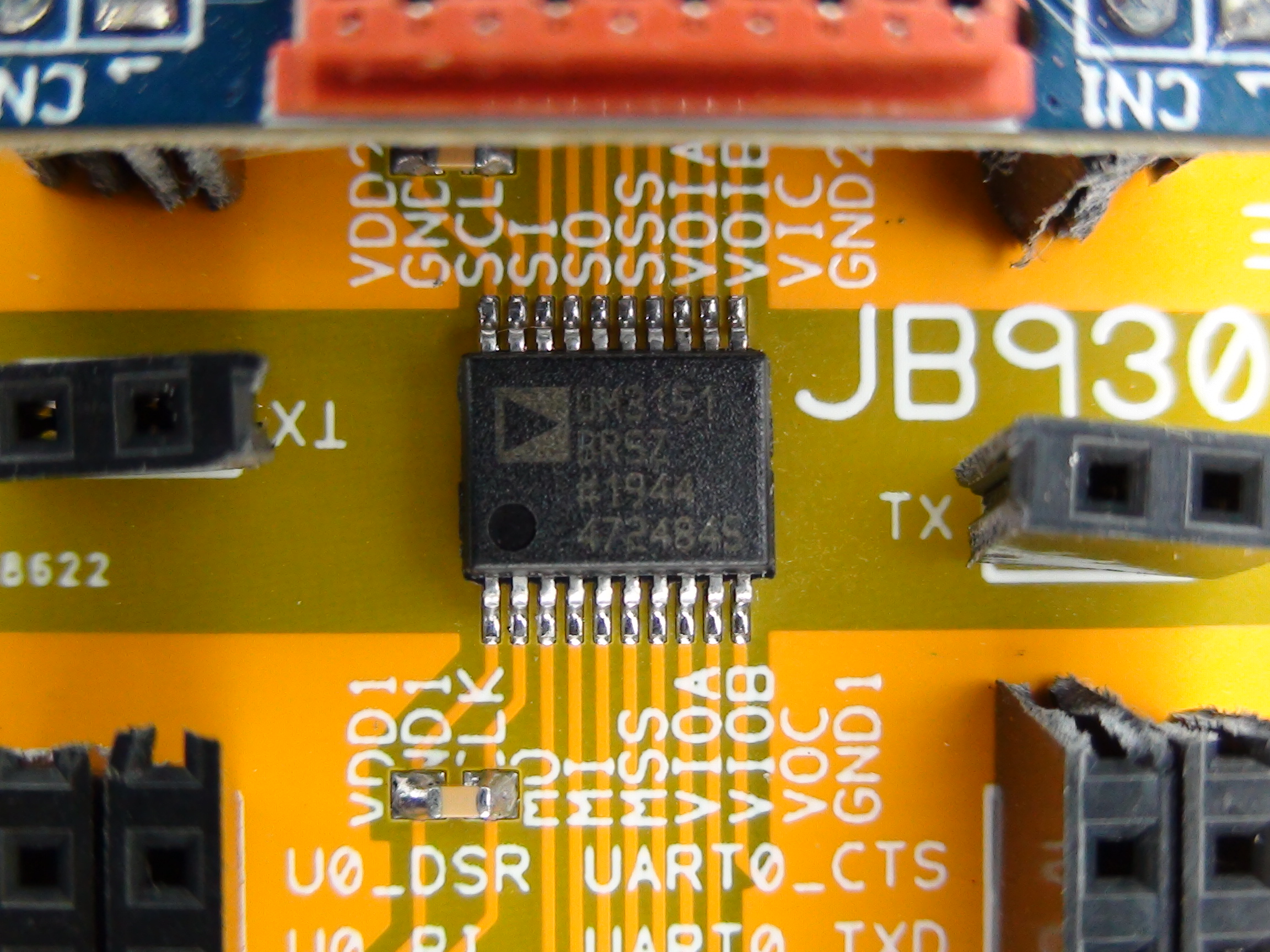
This board connects the SPI slave from one of the FT930s to the SPI master of the other FT930, through the SPI isolator. The isolator ensures the grounds of both boards remain disconnected from each other. There’s two ports at the edges, which connect directly to the SPI master and slave, for debugging use, and the connectors in-between are wired to the UART TX and RX pins.
The UMFTPD2A board is needed to program the FT930s. It includes a UART channel, which is very useful for debugging. A quick “Hello World” confirms the development boards are in working order.
In order to validate whether the SPI isolator is functioning, I uploaded the “SPI Slave Example 1” and “SPI Master Example 1”, from the FT9xx examples folder, to the development boards. No luck at first though, the data wasn’t coming through.
I changed the example to just test the GPIO function of the pins, toggling them on and off, and log their state through UART, on both sides. Then I measured the pins directly. The SPI master pins were transmitting correctly, the SPI slave pins were receiving correctly, but the SPI slave board was not seeing any incoming data, nor transmitting anything. The SPI isolator did appear to be working correctly, though.
After a bit of searching, I found my problem. While the FT930 does have only one SPI slave device, there are two possible pads to use it. Either pins 34 to 37, or pins 0 to 3. The example was using the former, I designed the wiring on my board to use the latter.
#define GPIO_SPIS_CLK 0
#define GPIO_SPIS_MISO 1
#define GPIO_SPIS_MOSI 2
#define GPIO_SPIS_SS 3
In addition to changing the pin numbers, I also had to change the function that the pins are set to. SPIS is function 2 on the former pad, while it’s function 1 on the latter.
gpio_function(GPIO_SPIS_CLK, pad0_spis0_clk);
gpio_function(GPIO_SPIS_SS, pad3_spis0_ss);
gpio_function(GPIO_SPIS_MOSI, pad2_spis0_mosi);
gpio_function(GPIO_SPIS_MISO, pad1_spis0_miso);
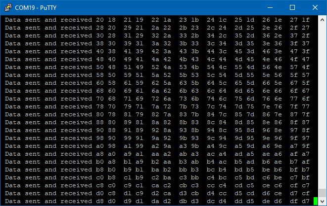
With these adjustments, the example application works as expected. Which validates that the soldered board is functioning as it should. Based on the datasheet of the isolator, the maximum SPI clock rate at 3.3V is 12.5MHz. This aligns well with the FT930 clock of 100MHz, using 8 as the SPI clock divider. The testing example appears to work reliably using this clock speed.
spi_init(SPIM, spi_dir_master, spi_mode_0, 8);
In the next post, I will explore how to set up the FT930 microcontrollers as USB audio devices.


JoSTC is een waardevol initiatief dat een professioneel platform biedt voor kennisdeling en discussie binnen de exportcontrol-gemeenschap. Het tijdschrift draagt bij aan beter begrip van regelgeving, naleving en internationale samenwerking. De betrokkenheid van academische instellingen, zoals Telkom University Jakarta, kan de kwaliteit van onderzoek en bewustwording rond exportcontrole verder versterken.